Layout
Great Lakes Control & Engineering were recently contracted with the task of developing a power monitoring system that would be applied in factories which deal with 3 phase power that could possess voltage imbalances and a poor power factor. Voltage imbalances damage delicate machinery which could be expensive to repair or replace. Poor power factors result in additional charges from power utilities.
Great Lakes Control & Engineering, experimented with the EXTECH 3-Phase Power Analyzer/ Datalogger as a solution to the problem. Although the device possesses vast functions for power grid monitoring, it lacks the ability to send notifications upon the detection of a voltage imbalance and log large amounts of data. Team 3 was tasked with developing a device which would replicate the functions of the Extech device and possess additional features to make up for its shortcomings.
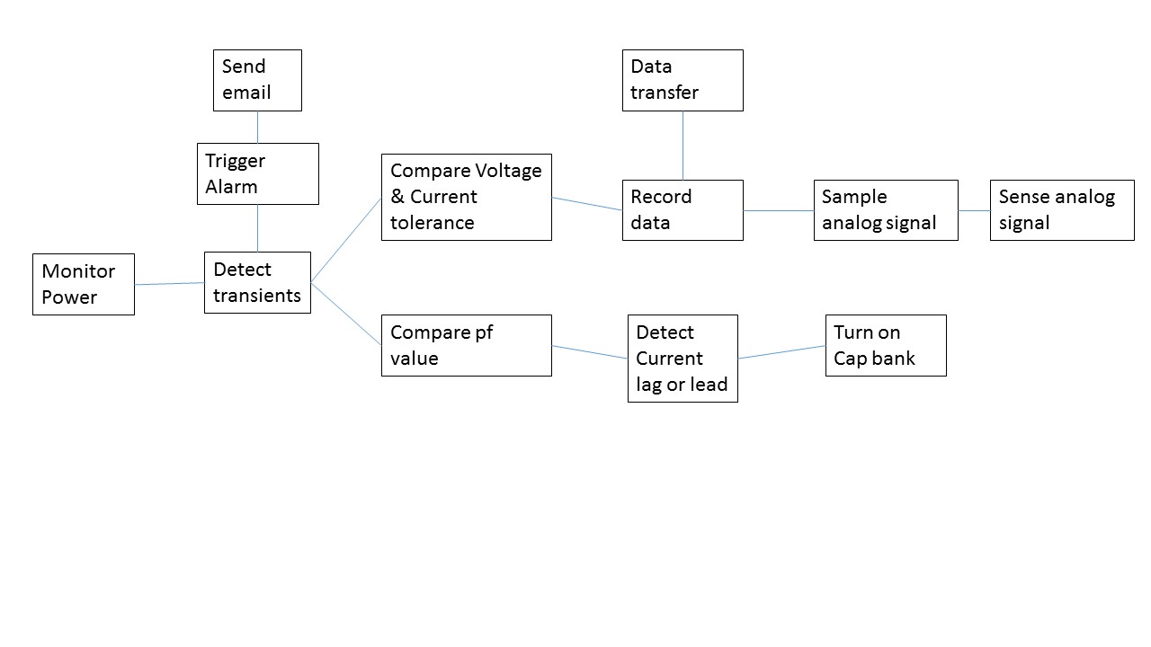
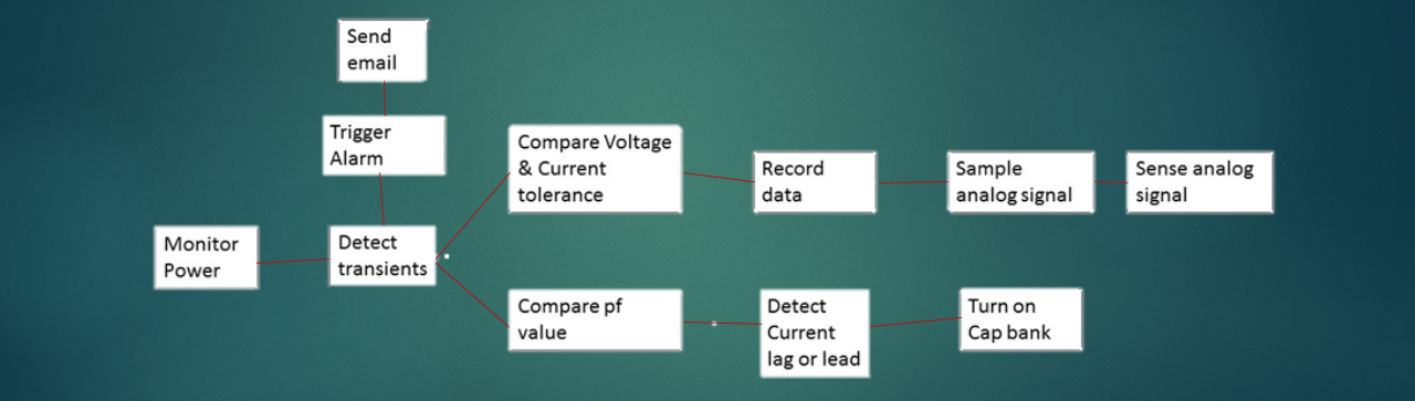
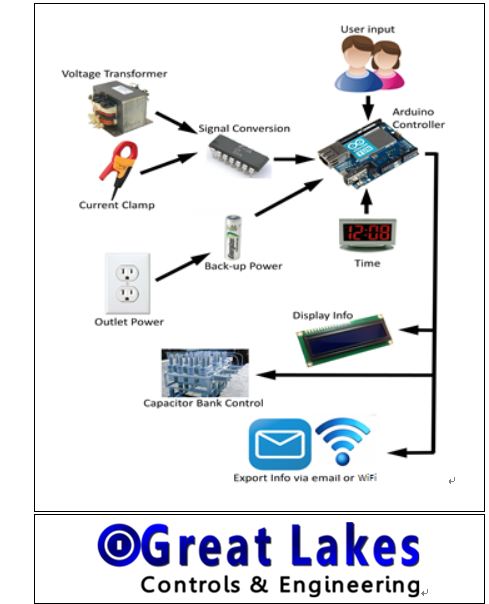
To meet the requirements set forth by our sponsor, we designed a device that would sense an analog power signal and log the data into the device’s internal memory. Afterwards, the device would compare the logged data with the set voltage and current tolerance values, and email a notification if the data is above the tolerance values. The email notification would also include a time stamp, and the current weather conditions at the factory’s location. The device would be equipped with two additional features: a capacitor bank control circuit that would switch on if the detected power factor is below the set tolerance and a backup battery that would be switched on upon the loss of power and send an email notification.
Great Lakes Control & Engineering were recently contracted with the task of developing a power monitoring system that would be applied in factories which deal with 3 phase power that could possess voltage imbalances and a poor power factor. Voltage imbalances damage delicate machinery which could be expensive to repair or replace. Poor power factors result in additional charges from power utilities.
Great Lakes Control & Engineering, experimented with the EXTECH 3-Phase Power Analyzer/ Datalogger as a solution to the problem. Although the device possesses vast functions for power grid monitoring, it lacks the ability to send notifications upon the detection of a voltage imbalance and log large amounts of data. Team 3 was tasked with developing a device which would replicate the functions of the Extech device and possess additional features to make up for its shortcomings.
To meet the requirements set forth by our sponsor, we designed a device that would sense an analog power signal and log the data into the device’s internal memory. Afterwards, the device would compare the logged data with the set voltage and current tolerance values, and email a notification if the data is above the tolerance values. The email notification would also include a time stamp, and the current weather conditions at the factory’s location. The device would be equipped with two additional features: a capacitor bank control circuit that would switch on if the detected power factor is below the set tolerance and a backup battery that would be switched on upon the loss of power and send an email notification.
Proposed Design Solution
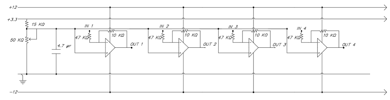
The most vital part of our design is the circuit’s ability to take an input voltage or current signal and convert it to a format our microcontroller can sample. Our microcontroller can only read voltages ranging from 0 to 5 V. To solve this issue, we designed a summing amplifier that would scale down the input signal and also add a 2.5V DC offset, which would enable us to properly see the sine wave of the voltage or current input signal.
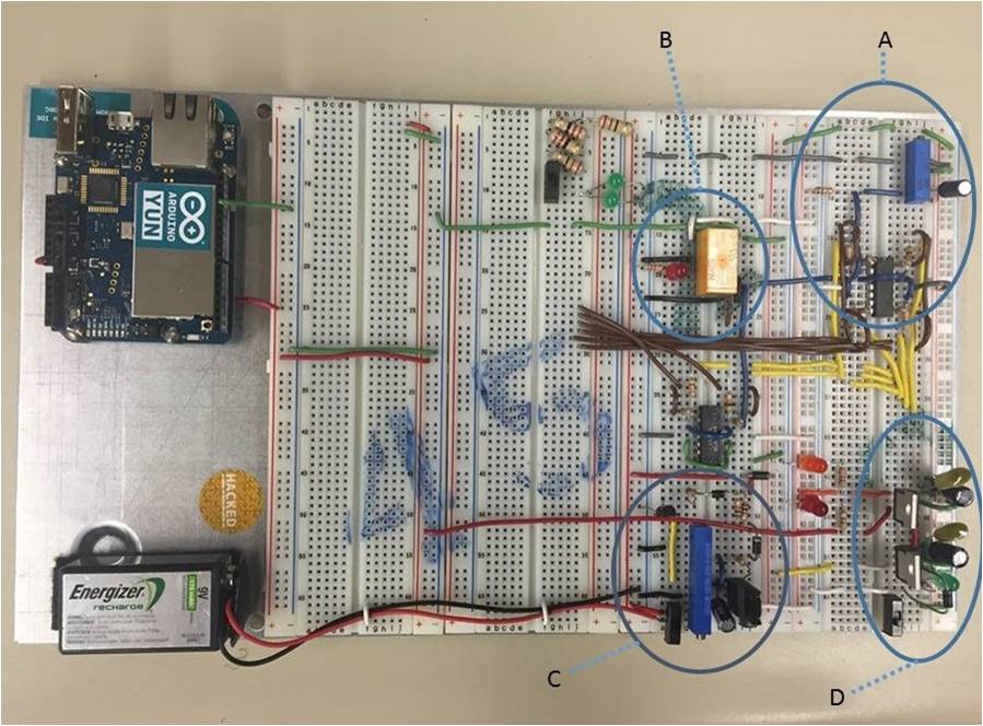
We plan to use transformers that will step down the signals to a 5 Vrms voltage; therefore, we will have an input of roughly 15 Vpp. If we build an inverting summer, the signal will be inverted which would not distort any information as long as each signal was inverted. We can also choose resistors such that the input signal is scaled down by a value of 4.7. If we are able to get a 5 Vpp input to the microcontroller, it would mean our input to the signal conversion circuit would be, 4.7*5= 23.5 Vpp, well suited to handle the expected 15 Vpp signal. We used to quad operational amplifiers to realize this design as can be seen in part A of figure above.
To create the DC offset, we used a voltage divider with a variable pot to grant us the ability to control the output offset through calibration. The input terminals of the operational amplifier have a high impedance so there is little concern of loading effects while using a voltage divider and to create a stiff voltage, we used capacitors tied to ground. The signal conversion circuit schematic can be found in figure below:
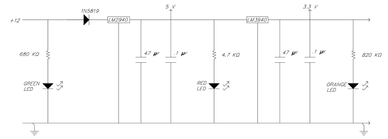
To power our circuit, we plan to use a 120AC/12VDC converter. However, our micro controller does not have an on board regulator and requires a regulated 5 VDC power supply. To accommodate this requirement, we built a circuit to provide a regulated 5 V and 3.3 V source incase if needed. The design comes from research and availability of parts from the ECE 480 class lab at Michigan State University. We added LEDs with current limiting resistors to give an indication of a voltage presence at the output of each voltage regulator. The circuit can be seen in part D of Figure 3 and the schematic for the circuit can be found in figure below:
Another major issue we wanted to overcome, not included in the design specifications, was the concern for a loss of power. The product is intended for use in a factory setting, where after it is installed, there could possibly be no human interaction other than when an alarm rings out. Therefore, if the unit undetectably loses power, any voltage or current transients would go unnoticed and no email notification will be sent. If no transients are suspected, no one will think to have any interaction with the product. As a resolution, we designed a back up battery with a charging circuit.
To build a battery charging circuit that would have an overcharge protection, we use the circuit in Figure below. We used an LM317 voltage regulator so that we could vary the output voltage using a potentiometer. If the voltage charging the battery gets too high, the zener diode will conduct and forward bias the transistor. When the transistor is forward biased, the output of the voltage regulator will drop and the diode at the top of the circuit will prevent the battery from backfeeding the regulator. We chose a 9 V rechargeable battery that has a nominal voltage of 8.4 V. The components and settings of the circuit were chosen such that the battery will charge to 8.6 V with a maximum current of 20 mA. These parameters came from research of the specifications of the battery charger designed for this battery.
We also included a discharge design in this circuit, which utilizes a switch to add a load to the battery for testing purposes. This is made of a series of four 22-Ω resistors.
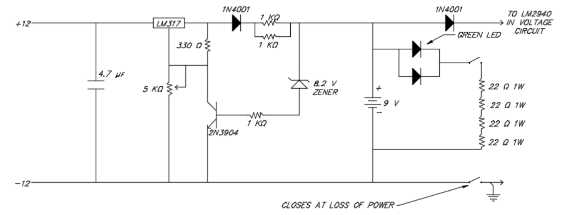
In order for the battery charger to work, a 24 V supply was needed. However, when the battery is required to power the circuit, the negative terminal must be connected to the circuit ground. To solve this issue, we used an undervoltage relay to close a contact that shorts the negative 12 V supply to ground when there is a loss of power. We also used a contact on the relay to turn on a red LED to signal the loss of input power. We plan to use inverted logic as an input to the micro controller to signal a loss of power. If the input is shorted to ground, external power is present, and if it is floating, there is a loss of power. The schematic for the circuit can be found in figure below and a picture can be seen in part B of device figure.
The microcontroller we selected for the project is the Arduino Yun. Although Arduino is seen as more of a hobbyist controller, given our short timeframe for the project and the inexperience of the team in terms of computer programming, this microcontroller serves as the best choice for multiple reasons. There are many open source codes and information on the internet pertaining to our project like for sending emails, writing to LCD displays, writing to USB, to name a few. This selected microcontroller also has 6 analog inputs for our signal sampling, an Ethernet port, microSD port, a USB port, and enough digital input/output ports to write to the LCD screens and our pushbutton inputs. With this controller, we can sample the signals, program any settings with the pushbuttons, save data to the microSD, send emails, and export data to a USB drive.
A limiting factor of our selected microcontroller was the number of inputs/outputs, as we would need a total of nine digital pins on the microcontroller in order to control the four LCD screens. Seeing as we would need pins for various applications, there was a need to reduce the number of pins used for the LCDs without reducing the number of LCD¡¯s. In order to do this we would have to use I2C communication, therefore, we would need to buy modules that allow the LCD¡¯s to use this form of communication by giving the LCD¡¯s an address, where no LCD shares the same address.
The major parts of our conceptual design that remain unfinished are the programming of the microcontroller to process the input signals, send emails, write data to either a USB or a microSD, and a clipping circuit to protect our product from large voltage or current transients.
The most vital part of our design is the circuit’s ability to take an input voltage or current signal and convert it to a format our microcontroller can sample. Our microcontroller can only read voltages ranging from 0 to 5 V. To solve this issue, we designed a summing amplifier that would scale down the input signal and also add a 2.5V DC offset, which would enable us to properly see the sine wave of the voltage or current input signal.
We plan to use transformers that will step down the signals to a 5 Vrms voltage; therefore, we will have an input of roughly 15 Vpp. If we build an inverting summer, the signal will be inverted which would not distort any information as long as each signal was inverted. We can also choose resistors such that the input signal is scaled down by a value of 4.7. If we are able to get a 5 Vpp input to the microcontroller, it would mean our input to the signal conversion circuit would be, 4.7*5= 23.5 Vpp, well suited to handle the expected 15 Vpp signal. We used to quad operational amplifiers to realize this design as can be seen in part A of figure above.
To create the DC offset, we used a voltage divider with a variable pot to grant us the ability to control the output offset through calibration. The input terminals of the operational amplifier have a high impedance so there is little concern of loading effects while using a voltage divider and to create a stiff voltage, we used capacitors tied to ground. The signal conversion circuit schematic can be found in figure below:
To power our circuit, we plan to use a 120AC/12VDC converter. However, our micro controller does not have an on board regulator and requires a regulated 5 VDC power supply. To accommodate this requirement, we built a circuit to provide a regulated 5 V and 3.3 V source incase if needed. The design comes from research and availability of parts from the ECE 480 class lab at Michigan State University. We added LEDs with current limiting resistors to give an indication of a voltage presence at the output of each voltage regulator. The circuit can be seen in part D of Figure 3 and the schematic for the circuit can be found in figure below:
Another major issue we wanted to overcome, not included in the design specifications, was the concern for a loss of power. The product is intended for use in a factory setting, where after it is installed, there could possibly be no human interaction other than when an alarm rings out. Therefore, if the unit undetectably loses power, any voltage or current transients would go unnoticed and no email notification will be sent. If no transients are suspected, no one will think to have any interaction with the product. As a resolution, we designed a back up battery with a charging circuit.
To build a battery charging circuit that would have an overcharge protection, we use the circuit in Figure below. We used an LM317 voltage regulator so that we could vary the output voltage using a potentiometer. If the voltage charging the battery gets too high, the zener diode will conduct and forward bias the transistor. When the transistor is forward biased, the output of the voltage regulator will drop and the diode at the top of the circuit will prevent the battery from backfeeding the regulator. We chose a 9 V rechargeable battery that has a nominal voltage of 8.4 V. The components and settings of the circuit were chosen such that the battery will charge to 8.6 V with a maximum current of 20 mA. These parameters came from research of the specifications of the battery charger designed for this battery.
We also included a discharge design in this circuit, which utilizes a switch to add a load to the battery for testing purposes. This is made of a series of four 22-Ω resistors.
In order for the battery charger to work, a 24 V supply was needed. However, when the battery is required to power the circuit, the negative terminal must be connected to the circuit ground. To solve this issue, we used an undervoltage relay to close a contact that shorts the negative 12 V supply to ground when there is a loss of power. We also used a contact on the relay to turn on a red LED to signal the loss of input power. We plan to use inverted logic as an input to the micro controller to signal a loss of power. If the input is shorted to ground, external power is present, and if it is floating, there is a loss of power. The schematic for the circuit can be found in figure below and a picture can be seen in part B of device figure.
The microcontroller we selected for the project is the Arduino Yun. Although Arduino is seen as more of a hobbyist controller, given our short timeframe for the project and the inexperience of the team in terms of computer programming, this microcontroller serves as the best choice for multiple reasons. There are many open source codes and information on the internet pertaining to our project like for sending emails, writing to LCD displays, writing to USB, to name a few. This selected microcontroller also has 6 analog inputs for our signal sampling, an Ethernet port, microSD port, a USB port, and enough digital input/output ports to write to the LCD screens and our pushbutton inputs. With this controller, we can sample the signals, program any settings with the pushbuttons, save data to the microSD, send emails, and export data to a USB drive.
A limiting factor of our selected microcontroller was the number of inputs/outputs, as we would need a total of nine digital pins on the microcontroller in order to control the four LCD screens. Seeing as we would need pins for various applications, there was a need to reduce the number of pins used for the LCDs without reducing the number of LCD¡¯s. In order to do this we would have to use I2C communication, therefore, we would need to buy modules that allow the LCD¡¯s to use this form of communication by giving the LCD¡¯s an address, where no LCD shares the same address.
The major parts of our conceptual design that remain unfinished are the programming of the microcontroller to process the input signals, send emails, write data to either a USB or a microSD, and a clipping circuit to protect our product from large voltage or current transients.
FAST Diagram