Pedro Rodriguez
ECE480
Application Note
Design Team 11
Power
System Overview and Buck Converter Operation
A
power system is needed in the Electronic Parachute Deployment (EPD) system to
convert the systems power source to the needed voltage potentials required by
the active components. This power system was developed after the key active
components in the design were chosen to ensure complete compatibility with the
rest of the system. The most significant challenge of this system design was
balancing efficiency, physical size, and cost. With the final power system
design the team has developed a system with a good balance of these design
criteria.
The
power system of the EPD must meet the voltage and current needs of the other
components within the system. The system needs three main outputs to the other
components of the system. It must provide a 5V output to both the analog
altimeter and the signal condition amplifier. The system also must output 3.3V
for the microcontroller. The last output is a short 2A burst output to power
the igniters.
The
power source chosen for this EDP system is a simple 9V battery. This is the
standard power device for commercial rocket altimeters and provides a large
amount of charge in a small physical space. Other options considered were a
Lithium ion coin cell battery. The 9V battery holds roughly five times the
amount of stored energy
Once
the power source was determined some power conversion was needed to change the
9V input to a 5V and 3.3V output. There are a few topologies that would allow
this step-down conversion. The system could use a linear voltage regulator, a
charge pump or a buck (step-down) converter. These power systems each are
unique and offer different benefits.
A linear voltage regulator is
typically quite cheap and usually requires two decoupling capacitors and the
voltage regulator itself to operate. These devices can take a voltage at a high
potential and output a lower voltage. This is done by dissipating excess
voltage as heat, and therefore is quite inefficient.
A charge pump system operates
by using a single integrated circuit that contains a series of switches and
capacitors. Within the IC the input voltage enters and then is passed between
capacitors using switches. These capacitors are to be sized in such a way that
the voltage can be increased or reduced at the output of the device. These
devices are more efficient than linear voltage regulators. The issue with
charge pumps is that all of your power must go through the IC, which has a
fixed amount of power it can handle. This usually limits the output current of
charge pumps to the milliamp range.
Finally there is the buck
converter topology. This topology is based around using an inductor as a
storage device. Figure 3.5.1 below
shows the basic design of the power system.
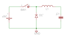
Figure 1
Simplified Buck Converter
When the switch in the
buck converter is closed, the inductor coil will charge up to Vin according to
the equation: ). This
assumes that the system started at 0V. This inductor will create a ¡®ramp¡¯ of
current that will go into the load assuming Vin is a constant. After a certain time, the switch will
open. The inductor will try and dissipate its stored energy out to the
capacitor and the load that would be hooked up in parallel to this capacitor.
This along with the fact that the switch is open will cause the node between
the diode and the inductor to be at a negative potential compared to ground.
This will forward bias the diode and allow an amount of charge to flow back
into the inductor. During a single switching cycle the amount of current
through the load capacitor (using Kirchhoff Current Law) would be equal to the
current out of the inductor minus the current going out to the load. If this
were to be calculated or graphed you could notice that average current that
flow through the capacitor would be 0V. Kirchhoff Current Law is used to
describe current entering a node at any instantaneous point in time. This Law
could be extended to show that the average current entering a node must be the
average current leaving the node. When this is now considered, assuming the
average current through the capacitor is 0V, and then the average current
through the inductor must equal the average current in the load.
). This
assumes that the system started at 0V. This inductor will create a ¡®ramp¡¯ of
current that will go into the load assuming Vin is a constant. After a certain time, the switch will
open. The inductor will try and dissipate its stored energy out to the
capacitor and the load that would be hooked up in parallel to this capacitor.
This along with the fact that the switch is open will cause the node between
the diode and the inductor to be at a negative potential compared to ground.
This will forward bias the diode and allow an amount of charge to flow back
into the inductor. During a single switching cycle the amount of current
through the load capacitor (using Kirchhoff Current Law) would be equal to the
current out of the inductor minus the current going out to the load. If this
were to be calculated or graphed you could notice that average current that
flow through the capacitor would be 0V. Kirchhoff Current Law is used to
describe current entering a node at any instantaneous point in time. This Law
could be extended to show that the average current entering a node must be the
average current leaving the node. When this is now considered, assuming the
average current through the capacitor is 0V, and then the average current
through the inductor must equal the average current in the load.
By
carefully regulating when the switch is opened and closed and by choosing the
inductor you will be able to store energy in the inductor and release it slowly
during discharge cycles. This allows the step-down of voltages with a
theoretical 100% efficiency. In real systems power loses will be seen mainly in
the inductor resistance, the gate resistance of a switch transistor (what is
typically used as the switch in this system), and the voltage drop over the
diode. Even with these loses the system can reach high level of efficiency in
the 90% range.
The
team initially chose to try and use a step-down (buck) converter to do this
power
conversion. This
converter would be quite efficient, but could be a bit more difficult to
implement. In buck converter system you can buy an integrated control that will
operate the switch and it will have some switching regulation control method.
Also buck-converter integrated circuits may also move a switching transistor or
the diode on to the chip, so less external parts are needed.
The
team initially looked at trying to use a two-output buck converter IC, for
example the TPS54386 from TI. This
single chip along with external components would then change our 9V input to a
5V and 3.3V output. These dual type buck converter chips from TI required many
external components and were quite complex. Using a dual buck converter system
to get both output voltages would require more physical area and could increase
the cost of the system. Another potential hazard is having the two inductors
form the different supply rails couple in some way causing instability.
It
was then determined to attempt to just use the buck converter system to output
the 5V rail. This conversion from 9V to 5V could then be made very efficient.
This would be beneficial to the overall efficiency because the two active
devices, the analog altimeter and its instrumentation amplifier, on average
require more current then the microcontroller running on the 3.3V rail.
With
the 9V to 5V conversion in mind we set out to find a buck-converter IC that
will be efficient, require few external components, and be fairly inexpensive.
Our first choice was Texas Instrument¡¯s TPS560200. This converter met all the
previous requirements, however when we received the chips the team realized
that a new criterion was needed. This ICs were very
small and would be difficult to solder by hand. So the team started searching
for another buck converter IC with a better package. A new converter that
looked promising was then found. This was the TPS62160 from Texas Instruments.
This part worked well initially, but when more thorough testing was done a
potential hazard was found. When testing this buck converter IC the team added
an increasing amount of output capacitance to the output of the system. This
was done while observing the effect of the total output capacitance on the
output voltage ripple. More output capacitance would result in less output
ripple which is desired in the EPD application. While increasing the output
capacitance, the team noticed that the IC would go unstable and into thermal
shutdown with an output capacitance greater than 220nF. At the point of
instability the output ripple was quite small. It was decided not to use this
IC knowing it has this stability issue. A third buck converter IC, Texas
Instrument¡¯s LM2574, was then tested thoroughly and no hazards were found. This
was found to be very robust, it required very few external components, and was
the cheapest solution we had tried, so this is the chip chosen to be in our
design.
With
the buck converter then 5V supply was created, but there still needed to be a
3.3V rail created. Applying the 5V rail into the linear voltage regulator
completed this objective. This method is not as efficient as the buck
converter, but is very cheap and requires a minimal number of parts. This
method does decrease the efficiency of the system, but the 3.3V power rail only
powers the MSP430. The MSP430 requires little current to operate so the power
dissipation in the linear voltage regulator is minimized. Initially the part
used for this voltage regulator was the LM3940 in a T220 package. This then was
changed in the final circuit revision to a LP2950, due to size and power needs.
The original LM3940 was quite bulky and had the ability to provide a large
amount of output current, which in our application was unused. The LP2950 was
nearly identical in functionality to the original voltage regulator, except
that it was smaller and had a limit of 100mA of output current. For the EPD
system application this new voltage regulator will work.
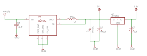
Figure
2: Our Final power schematic
This
designed power system provides a good mix of efficiency and cost for the EPD
system. With the way the system is designed the power source is also flexible
to allow voltages between 7 and 40 volts to be used. This feature was never
sought after in the design, but this does allow the system to provide good
voltage levels even when batteries lose their voltage potential slightly before
dying. More specifically the system could also be used with the 12V A23 type
battery that is fairly common. This power system has been in place through
violent rocket launch testing and still is holding up to the power needs of the
EPD system